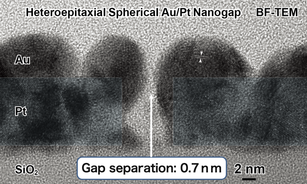
Core Tech: :Nanogap electrode chip with a gap separation of 0.7 nm
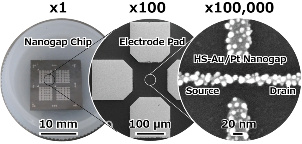
We use our own electron beam lithography (EBL) equipment to fabricate hundreds of platinum nanogap electrodes with a linewidth of 10 nm on a chip. To reduce their gap separations down to a few nm, the nanogap electrode chip are immersed in our unique heteroepitaxial spherical electroless gold plating (HS-ELGP) solution. We have established self-termination method of ELGP to control the gap separation of 0.7 nm without short circuit.
Core Tech: :Nano-combinatorial electrodes by electron-beam lithography
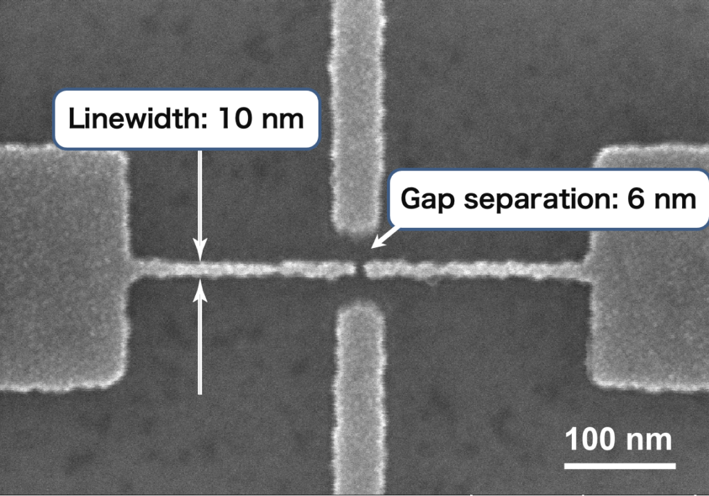
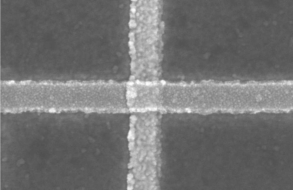
We have established the fabrication techniques of a platinum nanogap electrode by electron beam lithography (EBL) as shown in the SEM image. The linewidth and gap separation of Pt nanogap are 10 and 6 nm, respectively.
Using electron beam lithography equipment owned by our laboratory, various nanostructures could be designed by CAD, then drawn, deposited metals, and lifted off to fabricate 10-nm scale nano-combinatorial electrodes.
Platinum electrodes are heat resistant to 500°C
We are using this EBL technology to study nanoscale gas sensors, ferroelectric memory, and nanoscale ferromagnetic materials.
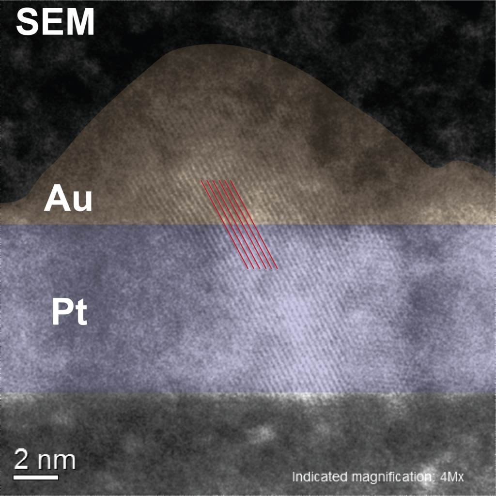
Electroless Au Plating (ELGP) is a nano-scale process on platinum (Pt) surfaces. The crystal lattice fringes (red parallel lines) are continuous at the Pt/Au interface as shown in the atomic resolution SEM image, indicating heteroepitaxial growth of Au on Pt surface.
This heteroepitaxial ELGP can be done in a safe solution at room temperature.
Gold can also be heteroepitaxially grown on Pd surfaces.
These nanoscale gold platings can be used as a seed layer for thicker plating.
Core Tech: :Nanogap electrodes prepared by self-terminating ELGP
Heteroepitaxial nano-scale ELGP on a platinum nanogap electrode allows to narrow the gap separation.
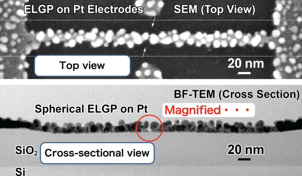
Here ELGP grow spherical gold on platinum nanogap. We could also grow uniform gold.
When the gap separation is narrowed less than a few nm, gold ions cannot reach between the gaps and the gold growth between the gaps self-terminate.
If we magnify the nanogap electrode fabricated by the self-terminating ELGP, heteroepitaxial spherical growth of gold on the initial platinum gap could be observed.
The gap separation of this nanogap electrode is 0.7 nm, which is equivalent to only three gold atoms.
Heteroepitaxial ELGP on Pt results in an extremely stable spherical nanostructure, and this nanogap electrodes is stable against annealing up to 200°C.
We are using this unique ELGP technology for researches on ultra-fast transistors and DNA sequencers.
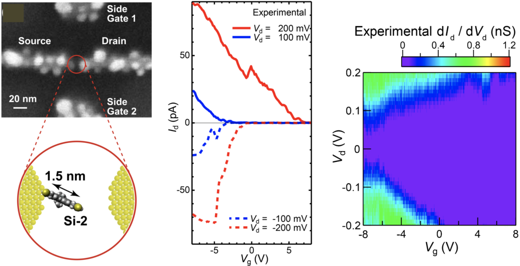
Theme 1: Ultra-fast transistors based on tunneling effect
Transistors with gate modulation of tunneling conduction can be realized using a nanometer-scale quantum dot and our heteroepitaxial spherical (HS-) Au/Pt nanogap electrodes.
Transistors that modulate tunneling conduction are expected to operate at ultra-high speeds because the tunneling process across between the electrodes below a femtosecond.
We have demonstrated a single-electron transistor with ideal Coulomb diamonds using a gold nanoparticle and the HS-Au/Pt nanogap electrodes, and reported three-input gate logic circuit operation.
We also demonstrated a single-molecule single-electron transistor operation using a π-conjugated molecule as a semiconductor.
Currently, we are developing ultrafast transistors using a semiconductor quantum dot and the nanogap.
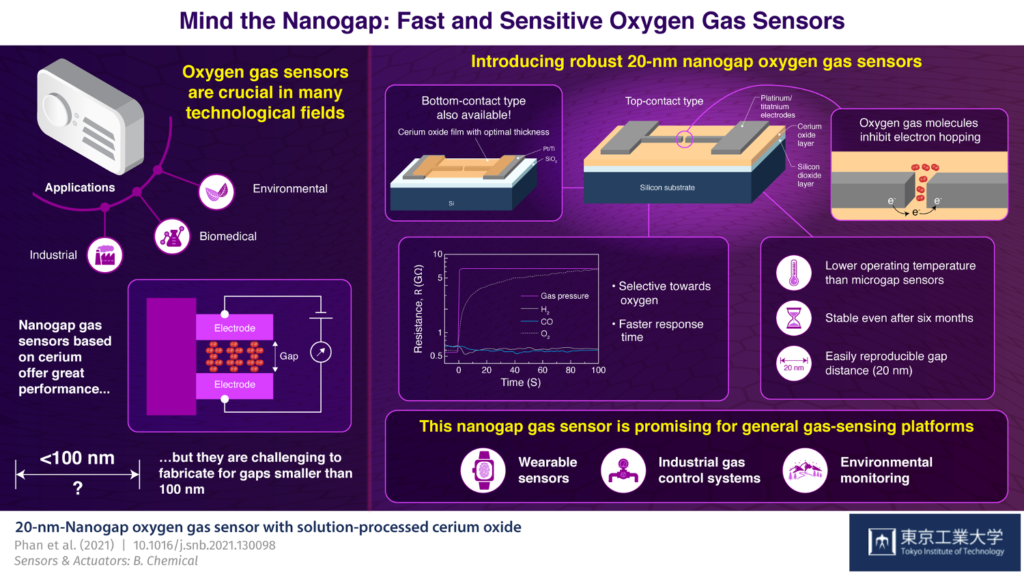
Theme 2: Nanogap gas sensors
Gas sensors have been manufactured on the micrometer scale
Resistance change-type gas sensors place an oxide semiconductor between a pair of electrodes and detect its electrical conduction depending on the gas atmosphere.
When our platinum nanogap electrodes with nanometer-scale gap separations are applied to resistance change-type gas sensors, we found that nanogap gas sensors show orders of magnitude faster response speeds than those of conventional sensors.
We are conducting research and development to apply this nanogap gas sensor technology to wearable gas sensors and ultra-low power consumption gas sensors.
Theme 3: ELGP nanopore DNA sequencer
Nanopore sequencers are a DNA sequencing method that reads changes in ion currents corresponding to single-stranded DNA passing through small pore (nanopore) of a few nm in size, and are attracting attention as a next-generation DNA sequencer that can decode long DNA.
Protein nanopores have been commercialized so far, but DNA sequencers using metal nanopores have not been realized.
We are developing a research project to realize an ELGP nanopore DNA sequencer by combining EBL, nano-electroless Au plating (ELGP) with self-termination method, and MEMS techniques.
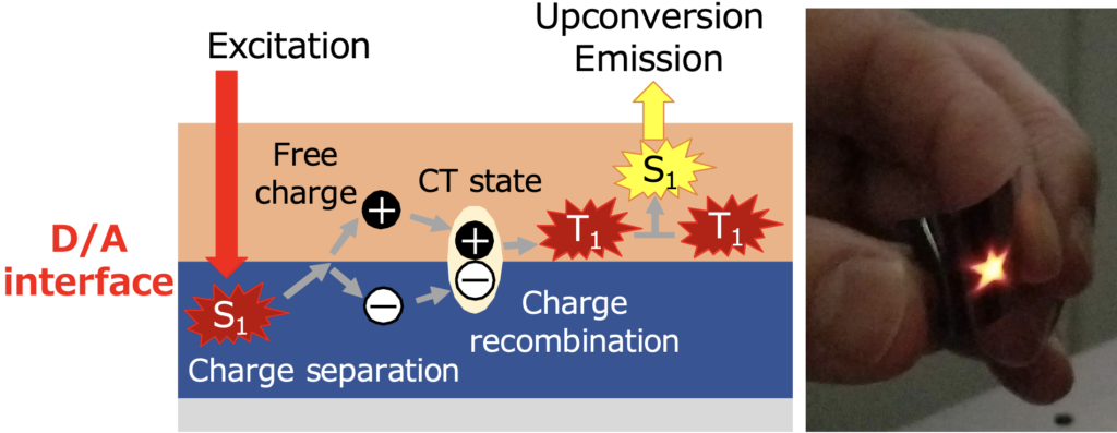
Theme 4: Efficient Photon Upconversion
We have developed for a novel method of photon upconversion (UC) by using charge separation and recombination that occurs at an organic semiconductor interface. When a singlet exciton reaches the solid-state interface between a donor and acceptor molecules, a pair of free charges are generated due to charge separation. After charge recombination, a triplet exciton forms at the interface, and subsequently a high energy singlet emission occurs after triplet-triplet annihilation. As shown in the right figure, when invisible near-infrared light is irradiated onto our organic thin film, yellow emission is produced; UC is expected to have applications in improving the efficiency of solar cells and in photodynamic therapy.
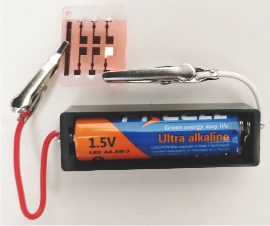
Theme 5: OLED (organic light-emitting diode) operated only by a 1.5 V battery
OLEDs are already in practical use in smartphones and televisions. However, the reduction of applied voltage required to emit light is a challenge for energy-saving displays. Recently, we have realized a novel working principle for OLED using an organic semiconductor interface. OLED can emit light only by connecting with a 1.5 V battery. This is the world’s lowest applied voltage for OLED, and we are working to further improvement of emission efficiency for practical use.
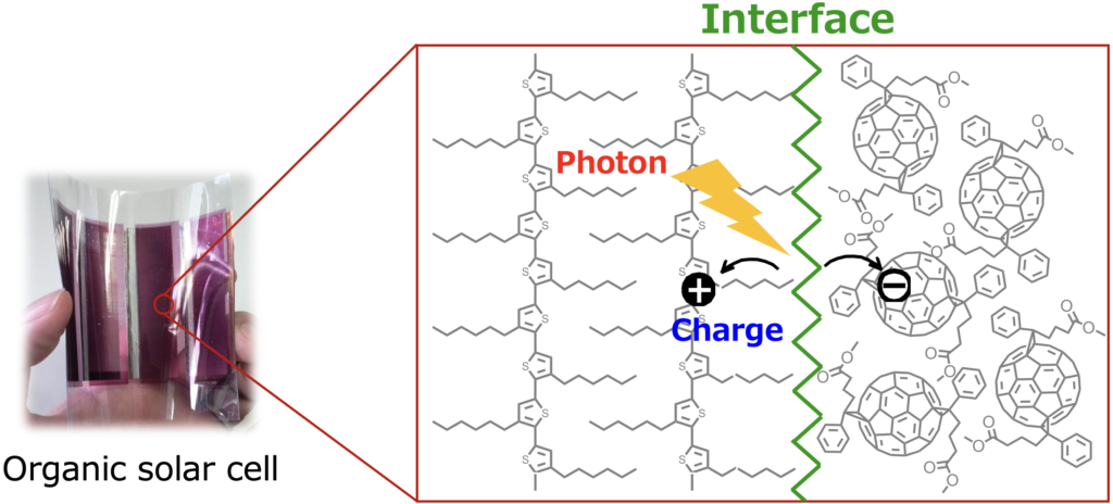
Theme 6: Control of interfacial structure for highly efficient organic solar cells
Organic solar cells are attracting much attention as an environmentally friendly next-generation energy conversion device. We aim to improve the efficiency of organic solar cells by revealing the mechanism of charge separation and recombination at the interface between donor and acceptor molecules.
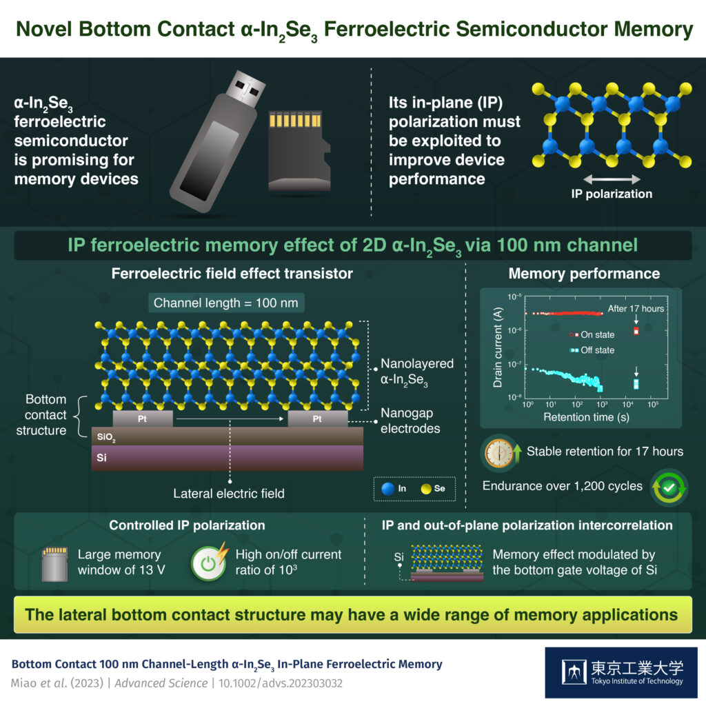
Traditional memory technologies face limitations in terms of speed, scalability, and power consumption, making them unsuitable for future data-intensive applications. Ferroelectric memory has garnered immense interest in recent years due to its potential for non-volatile storage, enabling data retention even when the power is turned off. The development of two-dimensional (2D) Van der Waals material α-In2Se3 has also opened new opportunities for advancing memory technologies.
We developed 2D ferroelectric semiconductor memory with a bottom contact 100 nm channel using in-plane polarization.
Theme 8: Nano-scale ferroelectric memory
Ferroelectric memory is a non-volatile memory that uses positive and negative residual polarization due to the hysteresis property of spontaneous polarization when an electric field is applied.
We are developing nanoscale ferroelectric memory by fabricating nano-combinatrial electrodes using EBLs.
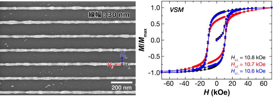
Theme 9: Nanostructure induced L10-ordering method for fabrication of ferromagnetic CoPt nanowires and their nano-spin devices
Ferromagnetic alloys with L10-ordered crystal structure such as CoPt and FePt exhibit large perpendicular magnetic anisotropy.
In L10 ferromagnetic crystals, two atoms are stacked alternately in the c-axis direction of the crystal, and the magnetic anisotropy energy (MAE) changes as the crystal lattice shrinks in the c-axis direction, resulting in large magnetic anisotropy.
Recently, we developed the nanostructure-induced L10 ordering method for ferromagnetic CoPt nanowires by crystalizing nanowire with extremely high internal stress. We also develop spin devices using the L10-CoPt nanowires.