“Developments of Extreme Nanofabrication Technologies and Functional Nanodevices”.
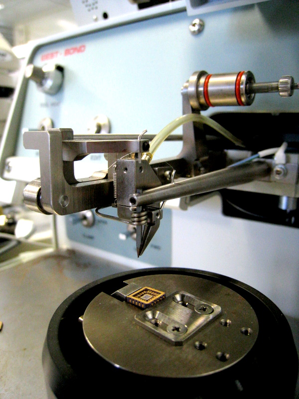
Our laboratory develops novel and various nanodevices such as ultra-fast transistors, nanogap gas sensors, DNA sequencers, ferroelectric memory, and nano-spintoronic devices by utilizing single-nanoscale structural control technology at the level of a few tens of atoms.
Our laboratory is capable of performing consistent operations from silicon wafer dicing to nanodevice fabrication and characterization.
Here, we will introduce basic nanodevice fabrication processes and evaluation methods, along with the experimental equipment.
動画再生
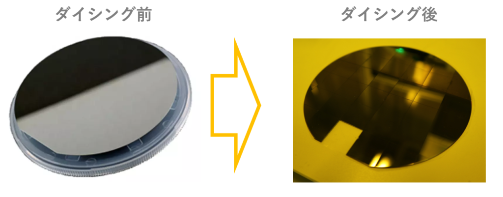
1. Dicing Silicon Wafer
Our nanodevices are fabricated on silicon wafers. Since they cannot be used in their original size, they are cut into 15 mm square pieces by a dicer (dicing saw) as substrates.
The substrate photo was taken in the yellow room. A yellow room is a clean room illuminated with yellow monochromatic light to prevent photosensitivity of resist. Subsequent processes are performed either in a clean room or in a yellow room.
2. Substrate Cleaning
Particles and contaminants on the substrate must be removed at a high level before nanodevices can be fabricated. Therefore, the substrates are always cleaned before processing. Substrates are cleaned frequently, not only at the beginning, but also between processes.
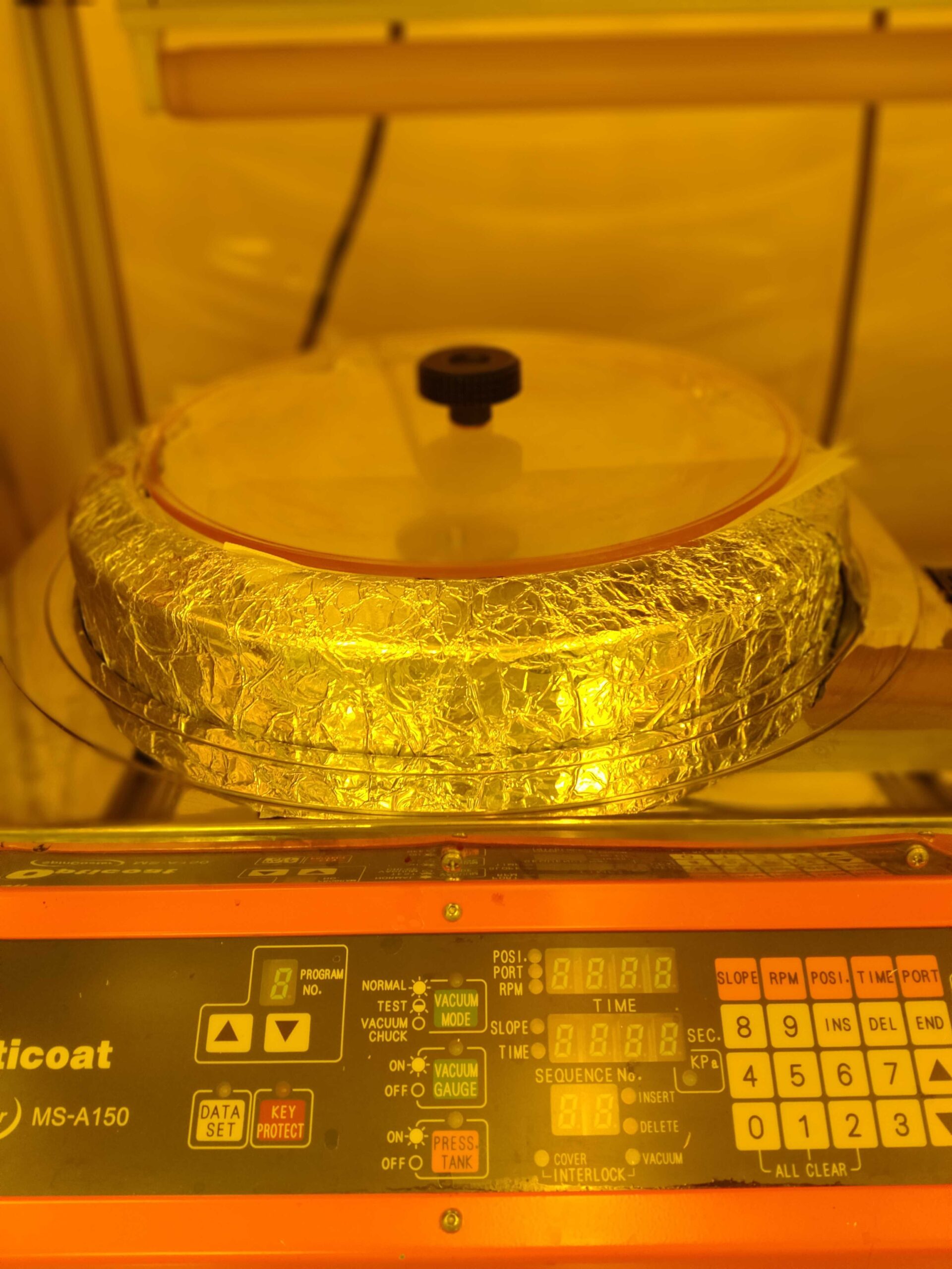
3. Resist Coating
A thin, uniform coating of polymer called resist (photosensitive material) is made by a spin coater. The spin coater spins the substrate at high speed to remove unnecessary resist. The resist film thickness is adjusted by the number of rotations.
Research Space
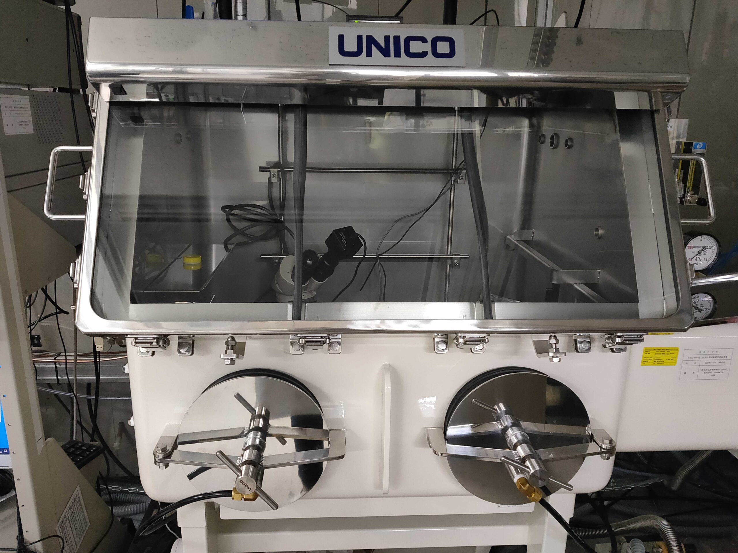
Majima Laboratory located R3 building, Suzukakedai-campus, Yokohama. We own a TFE electron beam lithography (EBL) system, an ultra-high resolution field emission scanning electron microscope (FE-SEM), an ultra-high vacuum molecular resolution scanning tunneling microscope (UHV-STM, three units), an ultra-high vacuum non-contact atomic force microscope (UHV-NC-AFM), an atomic force microscope with a horizontal dual magnetic field (AFM), and a physical and chemical property evaluation systems.
Experimental Equipments
Majima Laboratory has a TFE EBL system, an ultra-high resolution FE-SEM, six scanning probe microscopes, two sets of vacuum probers and semiconductor parameter analyzers, metal evaporators, organic thin film evaporators, etc.
Device fabrication processes are also available in the lab. The equipments required for everything from device fabrication to measurement and evaluation is world-class in performance. We make the best use of these equipments to promote our research.